- 您现在的位置:买卖IC网 > Sheet目录450 > ISL5416EVAL1 (Intersil)EVALUATION PLATFORM FOR ISL5416
�� �
�
�ISL5416�
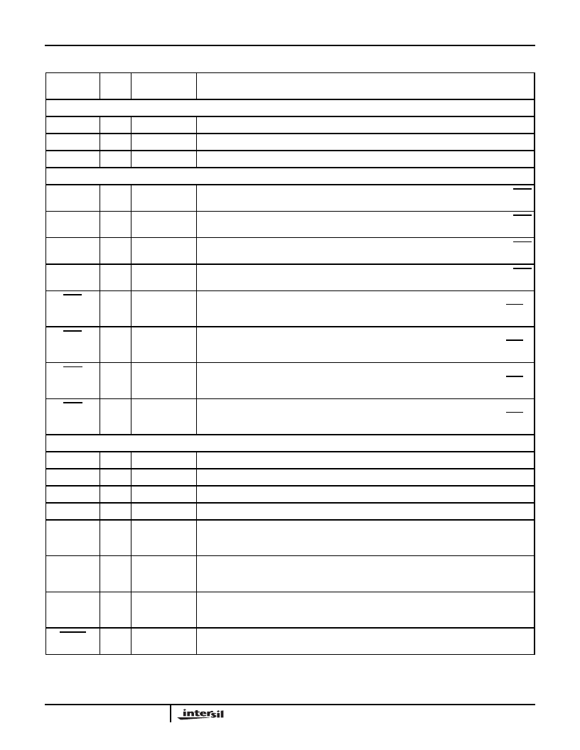
�Pin� Descriptions�
�INTERNAL�
�NAME�
�TYPE�
�PULL-UP/DOWN�
�DESCRIPTION�
�POWER� SUPPLY�
�Vcc�
�VccIO�
�GND�
�INPUTS�
�-�
�-�
�-�
�Positive� Power� Supply� Voltage� (core),� 1.8V� ±� 0.09�
�Positive� Power� Supply� Voltage� (I/O),� 3.3V� ±� 0.165�
�Ground,� 0V.�
�Ain(16:0)�
�I�
�PULL� DOWN�
�Parallel� Data� Input� bus� A.� Sampled� on� the� rising� or� falling� edge� (programmable)� of� clock� when� ENIA�
�is� active� (low).� The� bus� order� can� be� programmed� (See� IWA� =� 0*00h,� bit� 4).�
�Bin(16:0)�
�I�
�PULL� DOWN�
�Parallel� Data� Input� bus� B.� Sampled� on� the� rising� or� falling� edge� (programmable)� of� clock� when� ENIB�
�is� active� (low).� The� bus� order� can� be� programmed� (See� IWA� =� 0*00h,� bit� 4).�
�Cin(16:0)�
�I�
�PULL� DOWN�
�Parallel� Data� Input� bus� C.� Sampled� on� the� rising� or� falling� edge� (programmable)� of� clock� when� ENIC�
�is� active� (low).� The� bus� order� can� be� programmed� (See� IWA� =� 0*00h,� bit� 4).�
�Din(16:0)�
�I�
�PULL� DOWN�
�Parallel� Data� Input� bus� D.� Sampled� on� the� rising� or� falling� edge� (programmable)� of� clock� when� ENID�
�is� active� (low).� The� bus� order� can� be� programmed� (See� IWA� =� 0*00h,� bit� 4).�
�ENIA�
�I�
�PULL� DOWN�
�Input� enable� for� Parallel� Data� Input� bus� A.� Active� low.� This� pin� enables� the� input� to� the� part� in� one� of�
�two� modes,� gated� or� interpolated.� In� gated� mode,� one� sample� is� taken� per� CLK� when� ENIx� is�
�asserted.�
�ENIB�
�I�
�PULL� DOWN�
�Input� enable� for� Parallel� Data� Input� bus� B.� Active� low.� This� pin� enables� the� input� to� the� part� in� one� of�
�two� modes,� gated� or� interpolated.� In� gated� mode,� one� sample� is� taken� per� CLK� when� ENIx� is�
�asserted.�
�ENIC�
�I�
�PULL� DOWN�
�Input� enable� for� Parallel� Data� Input� bus� C.� Active� low.� This� pin� enables� the� input� to� the� part� in� one� of�
�two� modes,� gated� or� interpolated.� In� gated� mode,� one� sample� is� taken� per� CLK� when� ENIx� is�
�asserted.�
�ENID�
�I�
�PULL� DOWN�
�Input� enable� for� Parallel� Data� Input� bus� D.� Active� low.� This� pin� enables� the� input� to� the� part� in� one� of�
�two� modes,� gated� or� interpolated.� In� gated� mode,� one� sample� is� taken� per� CLK� when� ENIx� is�
�asserted.�
�CONTROL�
�CLKA�
�CLKB�
�CLKC�
�CLKD�
�SYNCIn1�
�I�
�I�
�I�
�I�
�I�
�PULL� DOWN�
�PULL� DOWN�
�PULL� DOWN�
�PULL� DOWN�
�Input� clock� for� data� bus� A.� CLKA� or� CLKC� may� be� used� for� Ain(16:0).�
�Input� clock� for� data� bus� B.� CLKB� or� CLKC� may� be� used� for� Bin(16:0).�
�Input� clock� for� data� bus� C.� CLKC� is� also� the� master� clock� for� all� channels� of� ISL5416�
�Input� clock� for� data� bus� D.� CLKD� or� CLKC� may� be� used� for� Din(16:0).�
�Global� synchronization� input� signal� 1.� SYNCIn1� can� update� the� carrier� NCOs,� reset� decimation�
�counters,� restart� the� filter,� and� restart� the� output� section� among� other� functions.� For� most� of� the�
�functional� blocks,� the� response� to� SYNCIn1� is� programmable� and� can� be� enabled� or� disabled.�
�SYNCIn2�
�I�
�PULL� DOWN�
�Global� synchronization� input� signal� 2.� SYNCIn2� can� update� the� carrier� NCOs,� reset� decimation�
�counters,� restart� the� filter,� and� restart� the� output� section� among� other� functions.� For� most� of� the�
�functional� blocks,� the� response� to� SYNCIn2� is� programmable� and� can� be� enabled� or� disabled.�
�SYNCO�
�O�
�Synchronization� Output� Signal.� The� processing� of� multiple� ISL5416� devices� can� be� synchronized� by�
�tying� the� SYNCO� from� one� ISL5416� device� (the� master)� to� the� SYNCIn� of� all� the� ISL5416� devices�
�(the� master� and� slaves).� An� optional� internal� SYNCO� to� SYNCInX� connection� is� provided.�
�RESET�
�I�
�PULL� UP�
�Reset� Signal.� Active� low.� Asserting� reset� will� halt� all� processing� and� set� certain� registers� to� default�
�values.�
�4�
�发布紧急采购,3分钟左右您将得到回复。
相关PDF资料
ISL55005IEZ-T7
IC AMP MMIC BIPO BROADBND SC70-6
ISL55007IEZ-T7
IC AMP MMIC BIPO BROADBND SC70-6
ISL55008IEZ-T7
IC AMP MMIC BIPO BROADBND SC70-6
ISL55009IEZ-T7
IC AMP MMIC BIPO BROADBND SC70-6
ISL55010IEZ-T7
IC AMP MMIC BIPO BROADBND SC70-6
ISL55011IEZ-T7
IC AMP MMIC BIPO BROADBND SC70-6
ISL55012IEZ-T7
IC AMP MMIC BIPO BROADBND SC70-6
ISL55013IEZ-T7
IC AMP MMIC BIPO BROADBND SC70-6
相关代理商/技术参数
ISL5416KI
功能描述:上下转换器 QUAD WIDEBAND DOWN CONVERTER, 256 CABGA RoHS:否 制造商:Texas Instruments 产品:Down Converters 射频:52 MHz to 78 MHz 中频:300 MHz LO频率: 功率增益: P1dB: 工作电源电压:1.8 V, 3.3 V 工作电源电流:120 mA 最大功率耗散:1 W 最大工作温度:+ 85 C 安装风格:SMD/SMT 封装 / 箱体:PQFP-128
ISL5416KIZ
制造商:Intersil Corporation 功能描述:LEAD-FREE QUAD WIDEBAND DOWN CONVERTER, 256 CABGA - Trays 制造商:Intersil Corporation 功能描述:PB-FREE W/ANNEAL QUAD DIGITAL DOWNCONVER 制造商:Intersil 功能描述:QD WIDEB& DWN CNVRTR 256 CABGA
ISL54200
制造商:INTERSIL 制造商全称:Intersil Corporation 功能描述:USB 2.0 High/Full Speed Multiplexer
ISL54200_07
制造商:INTERSIL 制造商全称:Intersil Corporation 功能描述:USB 2.0 High/Full Speed Multiplexer
ISL54200EVAL1Z
功能描述:EVALUATION BOARD FOR ISL54200 RoHS:是 类别:编程器,开发系统 >> 评估演示板和套件 系列:- 标准包装:1 系列:PCI Express® (PCIe) 主要目的:接口,收发器,PCI Express 嵌入式:- 已用 IC / 零件:DS80PCI800 主要属性:- 次要属性:- 已供物品:板
ISL54200IRUZ-T
功能描述:IC USB SWITCH DUAL SPDT 10UTQFN RoHS:是 类别:集成电路 (IC) >> 接口 - 模拟开关,多路复用器,多路分解器 系列:- 标准包装:2,500 系列:- 功能:视频交叉点开关 电路:1 x 8:6 导通状态电阻:- 电压电源:单电源 电压 - 电源,单路/双路(±):3.135 V ~ 5.25 V 电流 - 电源:55mA 工作温度:-40°C ~ 85°C 安装类型:表面贴装 封装/外壳:24-TSSOP(0.173",4.40mm 宽) 供应商设备封装:24-TSSOP 包装:带卷 (TR) 产品目录页面:1214 (CN2011-ZH PDF) 其它名称:FMS6502MTC24XTR
ISL54200IRZ
功能描述:IC USB SWITCH DUAL SPDT 10TDFN RoHS:是 类别:集成电路 (IC) >> 接口 - 模拟开关,多路复用器,多路分解器 系列:- 产品培训模块:Lead (SnPb) Finish for COTS
Obsolescence Mitigation Program 标准包装:36 系列:- 功能:多路复用器 电路:2 x 4:1 导通状态电阻:75 欧姆 电压电源:单/双电源 电压 - 电源,单路/双路(±):2 V ~ 12 V,±2 V ~ 6 V 电流 - 电源:- 工作温度:0°C ~ 70°C 安装类型:表面贴装 封装/外壳:20-SOIC(0.295",7.50mm 宽) 供应商设备封装:20-SOIC W 包装:管件
ISL54200IRZ-T
功能描述:IC USB SWITCH DUAL SPDT 10TDFN RoHS:是 类别:集成电路 (IC) >> 接口 - 模拟开关,多路复用器,多路分解器 系列:- 产品培训模块:Lead (SnPb) Finish for COTS
Obsolescence Mitigation Program 标准包装:36 系列:- 功能:多路复用器 电路:2 x 4:1 导通状态电阻:75 欧姆 电压电源:单/双电源 电压 - 电源,单路/双路(±):2 V ~ 12 V,±2 V ~ 6 V 电流 - 电源:- 工作温度:0°C ~ 70°C 安装类型:表面贴装 封装/外壳:20-SOIC(0.295",7.50mm 宽) 供应商设备封装:20-SOIC W 包装:管件